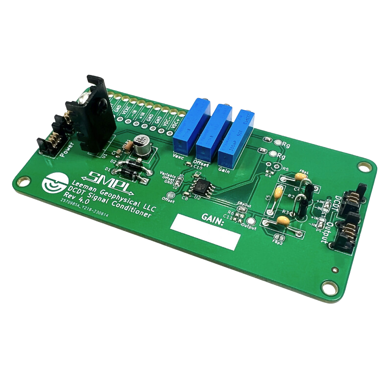
SMPL DCDT Signal Conditioner
This documentation covers part number 7-0000133
DCDTs or Direct Current Displacement Transducers are a very precise way to measure the displacement in a system based on the movement of a magnetically permeable core within a differential transformer. The transducer needs a stable input voltage as the output is proportional to the input. The output voltage range may need to be adjusted via the excitation voltage and/or an applied gain or offset to achieve the desired mapping of physical displacement to voltage.
The DCDT Signal Conditioner allows the interface of most DCDTs to the SMPL ecosystem with only minor adjustments needed to maximize the use of the digitizer's full dynamic range. With on-board gain and offset controls the signal can be amplified and offset to utilize a specific range of the DCDT's movement to make a single transducer even more versatile in a variety of scenarios.
Hookup
- Ensure all power is off. DO NOT power on the system until all steps of setup, including adjustment are complete, otherwise damage to the transducer may result!
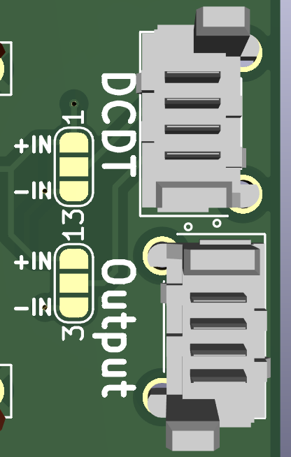
- Connect power to the PCB either via one of the two identical 4-pin SMPL connectors labeled power or via the through hole terminals GND, VDC-, and VDC+.
- Connect the transducer via either the 4-pin SMPL connector labeled DCDT or the through hole terminals GND, VEXC, -IN, and +IN. Reversing the input connections will reverse the sign of the output.
- Connect the output to the desired recording or measurement system via either the 4-pin SMPL connector or the through hole terminals GND, OUT.
- Proceed to the adjustment section BEFORE powering on the system or damage to your transducer may result!
Adjustment
Excitation Voltage
The excitation voltage of the circuit should be set to match the transducer's acceptable input voltage range as well as the excitation required to achieve the desired output voltages from the transducer. Adjustment of the output voltage range via the excitation voltage is always preferred to using gain as the noise of the output will be the least when no gain is applied.
- Ensure that power is off to the system.
- Setting the excitation voltage is most easily done with the transducer connected, but be sure that either the transducer can handle the full range of excitation voltages or that the Vexc potentiometer is turned all the way down (screw counter-clockwise until a click is heard or approximately 15 turns) before applying power to the system or damage to the transducer could result.
- Apply power to the system and measure the output excitation voltage using a multi-meter. This can be measured most easily at the GND and VEXC through hole terminals on the circuit board.
- Turn the potentiometer clockwise to increase the excitation voltage and counter clockwise to decrease it.
- Allow the unit to warm up under load for 30 minutes and repeat the adjustment.
As an example of determining a good starting point for the excitation voltage of a DCDT, we will consider a transducer from TransTek Inc. The transducer 0244-0000 is a +/- 1 inch range transducer. From the data table below we can see that at 6 VDC excitation it will output +/- 4.6 VDC at full scale and with 15 VDC excitation it will output +/- 12.1 VDC at full scale.
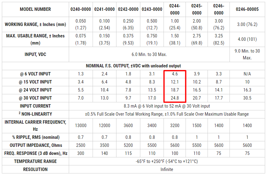
Suppose the system we want to connect to expects the full scale range to be represented by a range of 10 VDC (with no offset that is a +/- 5 VDC output). We can fit a line to the two data points from the datasheet to get equation:
From this equation we can calculate that an excitation voltage of 6.482 VDC will result in the desired output range from an ideal transducer. We may then set the excitation to a voltage of 6.48 VDC and proceed to test the output range in our system and adjust the excitation as necessary to dial in the required performance.
Gain and Offset
Gain applied to the transducer output and subsequent offset of the signal can be accomplished, but are considered advanced applications and covered in the Advanced Features section. Most applications are well served with no offset and a unity gain as the DCDT output voltage can be adjusted via the excitation as previously described. Therefore from the factory there is no gain or offset applied.
Testing
After the system has been connected and adjusted, move the transducer through the full range of motion and observe the output on a multi-meter or the data recording/digitization system. The output should vary in the desired voltage range corresponding to full scale movement of the DCDT. A calibration stand or ruler taped to the work surface may be helpful in moving the core of the DCDT more precisely.
Advanced Features
Applying Offset
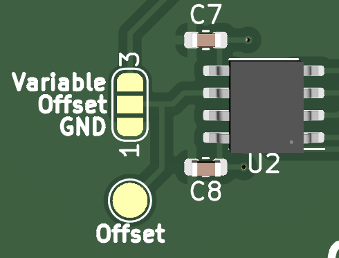
In some situations it may be desirable to offset the output of the system to work with a given digitizer or other constraint. The DCDT Signal Conditioner has the option to enable a variable offset allowing the zero output of the transducer to be set to nearly the full input voltage of the circuit. Typically this control is operated to offset the zero output to be within the range of -10 to 10 VDC.
To enable the offset feature, move the solder jumper labeled Offset from the GND pad to the Variable pad. Now turning the Offset potentiometer clockwise will increase the output offset and counter clockwise will decrease the offset. The offset voltage may be measured directly using the test point labeled Offset and any GND connection.
For example, consider the 0244-0000 transducer example from the excitation voltage adjustment section. The transducer was setup such that it produced a +/- 5 VDC output for the full scale +/- 1 inch range. Now suppose our recording and control system is only designed for an input of 0-10 VDC. The signal can be offset by +5 VDC to achieve the goal. The offset feature can also be used to create a false zero point. For example, if the desired output was 0 VDC when the transducer was at a physical location of +0.25 inches, the offset could be set to -1.25 VDC. Now the output of the transducer would be -6.25 to 3.75 VDC with the zero volt output corresponding to a position of 0.25 inches.
Applying Variable Gain
Some transducers may not produce a large enough output swing to maximize the full dynamic range of the digitizer or connected system. Variable gain can be applied to the signal to allow easy adjustment of the gain to optimize the transducer to system match.
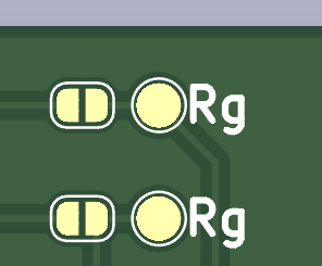
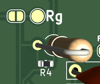
Two solder jumpers must be closed to enable the variable gain potentiometer. Once closed, the system will apply a gain set by the value of the potentiometer according to equation below. The value of the gain resistor can be measured by the two test points labeled Rg on the circuit board.
Gain can also be adjusted by setting the transducer at a known value (half full scale for example) and changing the potentiometer until the desired output is reached. Keep in mind that if an offset is being applied, it may be necessary to adjust these two controls multiple times to achieve both the desired gain and offset values. It may be easier to remove the offset, adjust the gain, then apply the offset again.
As an example, consider the 0240-0000 transducer from TransTek. This transducer will output 1.3 VDC at full scale when excited with 6 VDC. To increase that to a value of 10 VDC for a +/- 10 VDC output range we would need to apply a gain of 10 / 1.3 = 7.69 times. Plugging this value into the gain equation rearranged:
We can determine the gain resistor should be set to a value of 7.384kΩ. We can set the resistor, test, and make minor adjustments as necessary. Alternatively we can apply a fixed gain as described in the next section. There is a silkscreen printed area to write the applied gain value on for future reference on the front of the circuit board.
Applying Fixed Gain
Applying a fixed gain requires determining a gain resistor value and soldering it onto the circuit board, but has the advantage of being able to apply a very well known gain and reducing the effects of gain drift error from temperature changes modifying the resistance of the potentiometer used to apply a variable gain. This is the preferred method to apply gain, but requires additional parts and is not easily adjustable in system to accommodate transducer or requirement changes on the fly.
To apply a fixed gain, ensure that the solder jumpers for the variable gain potentiometer are NOT bridged. Calculate the resistor value needed to achieve the desired gain:
You'll need to then pick the closest standard value (E-Series) resistor to the calculated value. Checkout our handy explanation of the E-Series resistors over in this blog post. If you do not want the gain to be any higher than the ideal gain, err on choosing a resistor larger than the calculated value such that the gain would be slighlty less than the calculated gain.
We recommend using 1% or better resistors with low thermal coefficients for the best results. The resistor may be a through hole resistor and soldered into position R5 (standing on end) or an 0603 surface mount resistor soldered to position R4 on the circuit board. There is a silkscreen printed area to write the applied gain value on for future reference on the front of the circuit board.
Reversing Polarity
While many transducer manufacturers will specify an output polarity for their instruments, in some instances it is more useful for the output polarity of the system to be opposite. For example, if used as a feedback signal in a PID control system, the phasing of the actuator and feedback must be correct for effective control. Since the DCDT output is differential, we can switch the input connections to reverse the output polarity. While this can be accomplished by reversing the connections at the transducer, it can also be done by reversing the input connections using the polarity solder jumpers.
To reverse the input polarity change the solder bridge nearest the connector labeled DCDT to -IN and the jumper nearest the connector labeled Output to +IN. This will connect the nominally -IN pin to the +IN terminal of the instrumentation amplifier and the +IN pin to the -IN terminal.
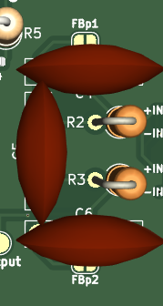
\paragraph{Input Filter Adjustment and Bypass}\mbox{}\
The mathematics of differential filters are discussed in the section on
filtering and should be referenced if modification of the stock filter is
required. The stock filter is a simple RC filter with a corner frequency for
differential signals of 2.2kHz and a common mode corner frequency of 6.6kHz. For
many displacement applications these are well above the expected mechanical
movement frequency of the system and simply help reduce noise on the signal from
high frequency sources. In some systems they may need to be modified to meet the
application's data acquisition requirements. To completely bypass the filters
the filter bypass jumpers by be bridged (FBp1 and FBp2).
Output Filter Adjustment and Bypass
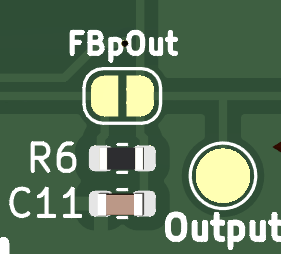
The analog output of the circuit is not filtered in any way. The output filter bypass jumper FBpOut is closed from the factory. If a low pass filter is desired it may be implemented after the output or resistor R6 and capacitor C11 may be populated to form a simple RC filter.
Troubleshooting
Issue: No change in output when transducer is moved.
- Verify that all connections are correct.
- Probe the Output test point with respect to ground. If signal is present, the issue is after the circuit or with the output connection itself.
- Verify that the input polarity solder jumpers are set (see Advanced Features).
- Verify that the offset solder jumper is set (see Advanced Features).
Issue: Offset potentiometer has no effect.
- Verify that the offset solder jumper is set to Variable (see Advanced Features).
Issue: Gain potentiometer has no effect.
- Verify that both Rg solder jumpers are closed (see Advanced Features).
Specifications
| Parameter | Min | Typ | Max | Unit |
| DC Input | ||||
| Voltage + | 13 | 15 | 17 | VDC |
| Voltage - | -13 | -15 | -17 | VDC |
| Current | - | - | - | mA |
| Transducer Excitation | ||||
| Voltage | - | - | - | VDC |
| Physical | ||||
| Weight | - | - | - | g |
| Width | - | - | - | mm |
| Length | - | - | - | mm |
| Height | - | - | - | mm |
Accessories
SMPL Cables
SMPL cables are the glue that holds the SMPL system together. These 4 pin cables are the backbone of the system and is based on the Molex Picoflex line of connectors.
Revisions
| Date | Changes |
| May 2024 | Moved Documentation to MkDocs Format |