SMPL Load Cell Signal Conditioner
This documentation covers part number 7-0000132/7-0000200
Overview
Introduction
Load cells are essential tools in laboratories and field systems, enabling precise weight or force measurements across a wide range, from a few grams to many tons. However, their low-level analog output, often just a few millivolts, poses a challenge for direct use in modern data acquisition systems.
The SMPL Load Cell Signal Conditioner solves this problem by amplifying and offsetting the load cell signal, allowing it to interface cleanly with DAQ systems, recorders, and other electronics. With adjustable gain and DC offset, the module makes it easy to scale the sensor output to match the full input range of your measurement system—often ±10 V—maximizing resolution and improving signal-to-noise ratio.
In addition to signal scaling, the board supplies clean, regulated excitation power to the load cell, critical for maintaining accurate and stable readings. Poor-quality excitation can introduce ripple and drift into your signal, so the SMPL board includes a precision onboard voltage reference.
Finally, common-mode and differential-mode input filtering provisions allow you to customize the system’s response using your RC components. Whether you're removing noise from the power supply, adding an anti-aliasing filter, or just smoothing out slow signals, the filtering section gives you full control. A free calculator is available to help select component values for your specific application.
What’s in the Box
When your unit arrives, unpack it and inspect all components for any shipping damage. If anything is missing or damaged, contact Leeman Geophysical immediately for a replacement.
Included:
- SMPL Load Cell Signal Conditioner (assembled PCBA)
Optional accessories such as cables and mounting hardware are available separately.
Specifications
| Parameter | Min | Typ | Max | Unit |
| DC Input | ||||
| Voltage + | 12 | 15 | 17 | VDC |
| Voltage - | -12 | -15 | -17 | VDC |
| Current (V+) No Transducer | - | 20 | - | mA |
| Current (V-) No Transducer | - | 17 | - | mA |
| Transducer Excitation | ||||
| Voltage | - | 5 | - | VDC |
| Physical | ||||
| Weight | - | 26 | - | g |
| Width | - | 50.8 | - | mm |
| Length | - | 101.6 | - | mm |
| Height | - | 12.7 | - | mm |
Connections
SMPL Connections
The SMPL Load Cell Signal Conditioner has four SMPL 4-wire connectors:
- A Power (x2) – Analog power input. These two connectors are electrically identical and allow power to be daisy-chained between multiple boards.
- Load Cell – Input from the load cell or other strain-based sensor.
- Output – Amplified and offset analog signal output.
The pinout for each connector is listed in the SMPL Standard section and is also printed on the back of the PCB using silkscreen labels for easy reference.
Through-Hole Solder Pad Connections
All signals are also broken out to strain-relieved through-hole pads on the upper left-hand corner of the board. These pads allow for direct wiring without the use of SMPL cables.
To use these:
- Insert the wire up through the open strain relief hole from the bottom of the board.
- Then insert the stripped end down through the corresponding solder pad.
- Solder the connection and pull the wire gently back down through the open hole to provide strain relief.
This method protects solder joints from vibration or accidental tugs on the wire.
Hookup Guide
-
Ensure all power is off.
⚠️ Do not power on the system until all setup and adjustments are complete. Powering the board too early may damage the transducer or circuit. -
Connect power to the PCB using one of the following methods:
- Either of the two 4-pin SMPL connectors labeled A Power
- Through-hole terminals: VDC+, VDC-, and GND
-
Connect the load cell using:
- The 4-pin SMPL connector labeled Load Cell, or
- Through-hole terminals: VExc+, VExc-, IN+, and IN-
(Note: Reversing IN+ and IN- will invert the output signal polarity.)
-
Connect the output to your data acquisition or measurement system using:
- The 4-pin SMPL connector labeled Output, or
- Through-hole terminals: OUT and GND
- Continue to the Adjustment Procedures section before applying power.
Adjustment Procedures
The two primary parameters you’ll need to configure on the SMPL Load Cell Signal Conditioner are gain and offset. These allow you to scale and shift the load cell signal to match the input range of your data acquisition system.
- Gain controls how much the input signal is amplified.
- Offset shifts the entire signal up or down by a fixed DC voltage.
These should be set during initial setup and may be fine-tuned depending on your specific sensor and DAQ system.
Gain Adjustment Procedure
In the default configuration, gain is controlled by a potentiometer labeled Gain on the PCB. You can also configure the system for a fixed gain using resistors.
Variable Gain Adjustment (Default)
The default potentiometer-based gain setting allows adjustment over a typical range of approximately 240x to 1100x, suitable for many common load cells. If you require a custom adjustment range, please contact us for a custom board suited to your application.
If the circuit board was previously configured for fixed gain, you’ll need to remove any resistors installed at R1 or R2, and re-close the two solder jumpers near R9 to re-enable the variable gain circuit.
Steps:
- Ensure the system is fully connected as described in the Hookup Guide.
- Power on the system and monitor the output using a multimeter or DAQ input.
- Apply a known load to the load cell or sensor. If you have a precision millivolt source, it may be used as well.
- Adjust the Gain potentiometer:
- Turn clockwise to increase gain.
- Turn counterclockwise to decrease gain.
- Continue adjusting until the output voltage matches the expected value based on your known input.
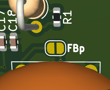
The effective gain of the system can be measured across the test points labeled Rg on the PCB. These test points represent the resistance controlling the gain of the instrumentation amplifier—either set by the onboard potentiometer or fixed resistors R1 and R2 (see Fixed Gain Configuration).
🛑 Note: Always ensure the circuit is unpowered before measuring resistance across the Rg test points. Measuring while powered may damage your multimeter or produce incorrect results. The effective gain of the system can then be calculated using the transfer function.
Fixed Gain Configuration
For applications requiring a more stable and known gain value (less susceptible to temperature drift), you can disable the variable gain and set a fixed gain using resistors.
You'll need to then pick the closest standard value (E-Series) resistor to the calculated value. Checkout our handy explanation of the E-Series resistors over in this blog post. If you do not want the gain to be any higher than the ideal gain, err on choosing a resistor larger than the calculated value such that the gain would be slighlty less than the calculated gain.
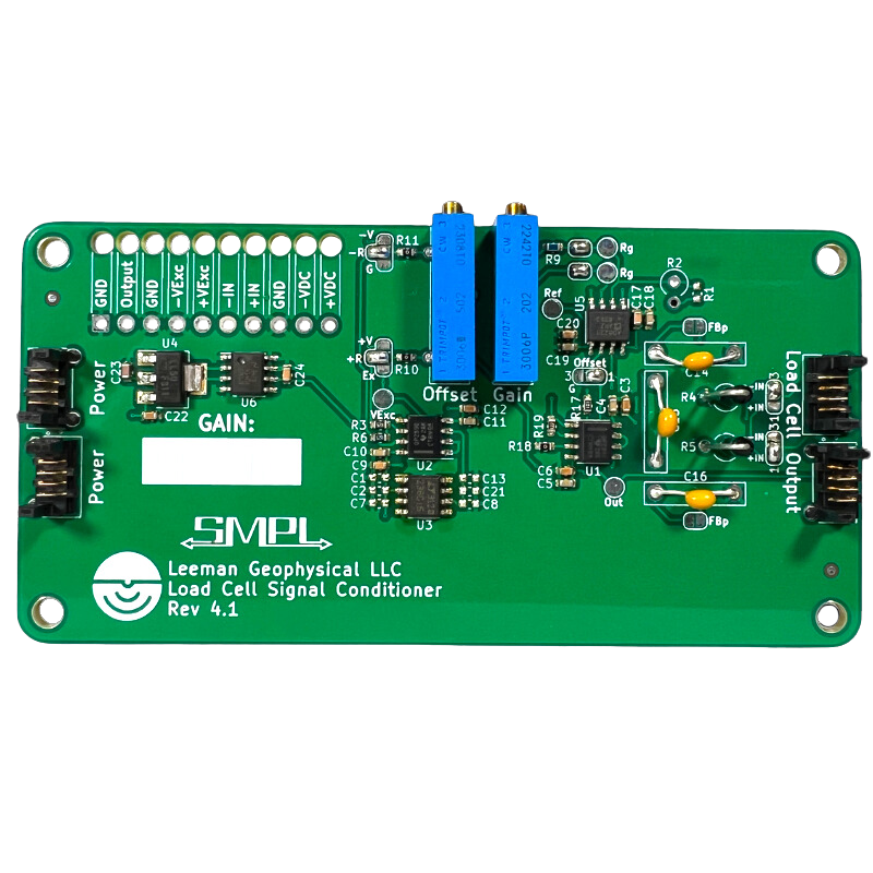
We recommend using 1% or better resistors with low thermal coefficients for the best results. The resistor may be a through hole resistor and soldered into position R2 (standing on end) or an 0603 surface mount resistor soldered to position R1 on the circuit board. There is a silkscreen printed area to write the applied gain value on for future reference on the front of the circuit board.
To disable variable gain:
Remove solder bridges on the two jumpers adjacent to the potentiometer, near component R9.

Remove the two solder bridge jumpers near R9 to disable variable gain. This enables the use of a fixed gain resistor at R1 or R2. The resulting gain resistance can still be measured across the test points labeled Rg.
To set a fixed gain:
- Populate either of the following:
- R1: 0603 surface-mount resistor
- R2: Axial through-hole resistor (vertical mount)
Both positions are in parallel and serve the same purpose—use whichever is more convenient.
Fixed gain can be set by populating the axial resistor footprint R2 or the 0603 surface mount footprint R1.
Transfer Function
Where:
- \(G\) is the voltage gain
- \(R_g\) is the total resistance between the two gain nodes
Offset Adjustment Procedure
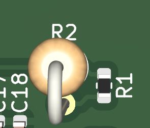
By default, the offset feature is disabled when you receive your board. To enable it, move the solder jumper labeled Offset from the GND (3) pad to the Variable (1) pad.

Offset jumper on the PCB. Bridge connections 3 and 2 for no offset. Bridge connections 2 and 1 for variable offset.
Once enabled, the Offset potentiometer allows you to apply a DC offset to the output signal:
- Turning the potentiometer clockwise increases the offset voltage.
- Turning it counterclockwise decreases the offset voltage.
🔧 Tip: Always adjust the system gain first, then apply offset. The final output offset is affected by the gain setting, so changing gain after offset may require re-adjustment.
Setting the Offset Voltage Range
Two 3-position solder jumpers near the Offset potentiometer define the minimum and maximum voltage that the potentiometer can apply.
Two 3-position jumpers near the offset potentiometer define the minimum and maximum offset voltage range. The top jumper sets the lower limit (default –1.024 V), and the bottom jumper sets the upper limit (default +1.024 V).
Minimum Offset Voltage
- Set by the top jumper nearest the PCB's edge
- Default: –R (–1.024 V reference voltage)
- Optional settings:
- G — 0 V (ground)
- –V — Negative system supply voltage
- ⚠️ Recommended to leave at –R unless a larger negative offset range is required. The reference voltage is the most stable.
Maximum Offset Voltage
- Set by the bottom jumper nearest the PCB's center
- Default: +R (+1.024 V reference voltage)
- Optional settings:
- EX — 5 V excitation voltage to the load cell
- +V — Positive system supply voltage
- ⚠️ Recommended to leave at +R unless your application requires a wider offset swing. The reference is again the most stable and predictable.
These jumpers allow you to customize the offset range for your system for maximum flexibility.
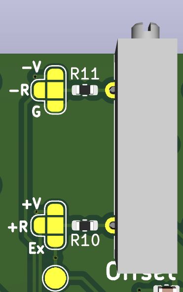
Reversing Polarity
If the output signal from your load cell is inverted from what you expect, you can reverse the polarity in hardware using onboard solder jumpers—no rewiring required.
To do this, move the two solder jumpers near the Load Cell and Output connectors to the opposite positions they are in. This swaps the signal polarity by routing the sensor’s +IN to the amplifier’s –IN input, and vice versa, effectively inverting the output voltage.
This feature is helpful if your system interprets tension as compression (or vice versa), or if your load cell was wired with reversed signal polarity.
Input polarity of the transducer can be reversed by moving the solder bridges on the jumpers to the positions closest to the centerline of the PCB.
Using the Output Filter
The SMPL Load Cell Signal Conditioner includes an optional passive low-pass filter on the output of the system, after all amplification and offset stages. This filter helps suppress high-frequency noise and improve signal quality, especially when long cables or sensitive digitizers are used.
The output filter consists of: - Two series resistors - Three capacitors
These components form both a differential-mode and common-mode RC low-pass filter.
Default Filter Configuration
The board is shipped with the following default components installed:
- Resistors: 240 Ω
- Capacitors: 0.1 µF
This configuration provides:
- Differential-mode corner frequency: ~2.2 kHz
- Common-mode corner frequency: ~6.6 kHz
You can easily modify the filter characteristics by replacing the resistors and/or capacitors. To do so, desolder the default components and solder in new values based on your desired cutoff frequency.
A free calculator is available to help determine the appropriate component values for your application: SMPL Filter Calculator (Google Sheets)
Bypassing the Filter
If output filtering is not needed, if you are troubleshooting, or using your own external filtering, the onboard filter can be bypassed. Close the two filter bypass jumpers located adjacent to the filter components to short the resistors and bypass the RC network entirely.
The output filter section includes two resistors and three capacitors forming common and differential low-pass filters. Close the adjacent solder jumpers to bypass the filter entirely.
Recommendation: For many systems, the default filter offers a good balance of noise reduction and signal speed. Only bypass or modify the filter if your application requires a different response.
Troubleshooting
Having trouble with your signal? This section covers common issues and how to resolve them.
No Change in Output When Load is Applied
- Check all wiring connections — Ensure power, load cell, and output cables are fully inserted or correctly soldered.
- Measure the Output test point relative to GND — If a signal is present here but not at your DAQ or meter, the issue is likely with the output wiring or the receiving device.
- Ensure the offset of the system has been set correctly or remove the offset feature for testing.
- Confirm the load cell is receiving excitation voltage — Measure the voltage between VExc+ and VExc–. It should be close to 5 V.
- Check for a faulty or overloaded sensor — If possible, test your load cell with a known working signal conditioner or simulate its output.
Offset Potentiometer Has No Effect
- Ensure the offset jumper is set to Variable — See Offset Adjustment Procedure.
- Confirm the offset range jumpers are correctly set.
Gain Potentiometer Has No Effect
- Confirm both Rg jumpers are closed — These enable the onboard variable gain circuit. See Gain Adjustment Procedure.
- Inspect R1 and R2 for residual solder or partially installed resistors — Leftover fixed-gain components can interfere with the potentiometer.
- Ensure the system is powered during testing — The gain control only affects the output when the circuit is active.
- Power off the circuit and measure Rg — If resistance does not change when adjusting the potentiometer, it may be damaged or disconnected.
General Troubleshooting Tips
- Double-check your power supply — Make sure it meets the required voltage and current specifications. Unstable or low supply voltage can cause erratic behavior.
- Use a known, testable load — Apply a repeatable, known weight or force to confirm system functionality before field use.
- Inspect for solder bridges or cold joints — This is especially important if you've modified jumpers, installed filtering components, or changed gain settings.
- Reset to default jumper settings — If you're unsure of the current configuration, return all jumpers to their documented default positions.
If you are still experiencing issues after completing these checks, contact support for assistance. We're happy to help troubleshoot your setup.
Board Revisions and Compatibility
All circuit boards labeled Revision 5.0 or later are fully compliant with the SMPL connector standard and follow the pinout and configuration described in this documentation.
Earlier versions of the Load Cell Signal Conditioner board (pre-5.0) may have: - Minor differences in SMPL connector pinout - Different default jumper configurations - Component value variations in filter or gain stages
If you are using a board without a visible revision label, or one marked as an earlier revision, please contact support for assistance in identifying and configuring your board correctly.
Revisions
| Date | Changes |
| May 2025 | Update and clarify documentation |
| May 2024 | Moved Documentation to MkDocs Format |